Product Summary
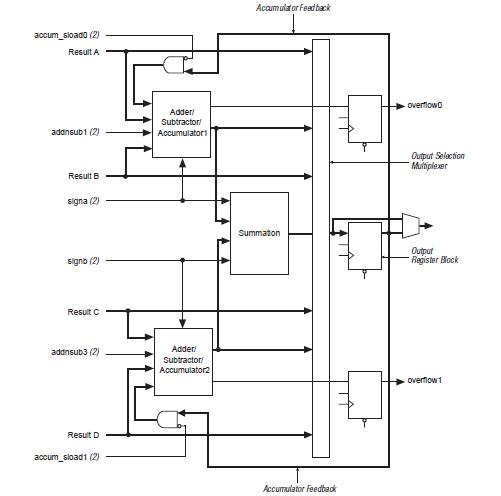
The EP1S10F672C7 is an FPGA. It is based on a 1.5-V, 0.13-μm, all-layer copper SRAM process, with densities of up to 79,040 logic elements (LEs) and up to 7.5 Mbits of RAM. The EP1S10F672C7 offers up to 22 digital signal processing (DSP) blocks with up to 176 (9-bit × 9-bit) embedded multipliers, optimized for DSP applications that enable efficient implementation of high-performance filters and multipliers. The EP1S10F672C7 supports various I/O standards and also offer a complete clock management solution with its hierarchical clock structure with up to 420-MHz performance and up to 12 phase-locked loops (PLLs).
Parametrics
EP1S10F672C7 absolute maximum ratings: (1)Supply voltage With respect to ground:–0.5 to 2.4 V or –0.5 to 4.6 V; (2)DC input voltage:–0.5 to 4.6 V; (3)DC output current, per pin :–25 to 40 mA; (4)Storage temperature No bias: –65 to 150 ℃; (5)Junction temperature BGA packages under bias:135 ℃.
Features
EP1S10F672C7 features: (1)Support for 66-MHz PCI (64 and 32 bit) in -6 and faster speed grade devices, support for 33-MHz PCI (64 and 32 bit) in -8 and faster speed-grade devices; (2)Support for 133-MHz PCI-X 1.0 in -5 speed-grade devices; (3)Support for 100-MHz PCI-X 1.0 in -6 and faster speed-grade devices; (4)Support for 66-MHz PCI-X 1.0 in -7 speed-grade devices; (5)Support for multiple intellectual property megafunctions from Altera MegaCoreR functions and Altera Megafunction Partners Program (AMPPSM) megafunctions; (6)Support for remote configuration updates; (7)10,570 to 79,040 LEs; (8)Up to 7,427,520 RAM bits (928,440 bytes) available without reducing logic resources.
Diagrams

| Image | Part No | Mfg | Description |  |
Pricing (USD) |
Quantity | ||||||
|---|---|---|---|---|---|---|---|---|---|---|---|---|
 |
 EP1S10F672C7 |
 |
 IC STRATIX FPGA 10K LE 672-FBGA |
 Data Sheet |

|
|
||||||
 EP1S10F672C7N |
 |
 IC STRATIX FPGA 10K LE 672-FBGA |
 Data Sheet |

|
|
|||||||
 (China (Mainland))


